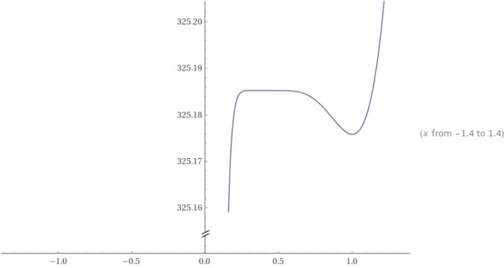
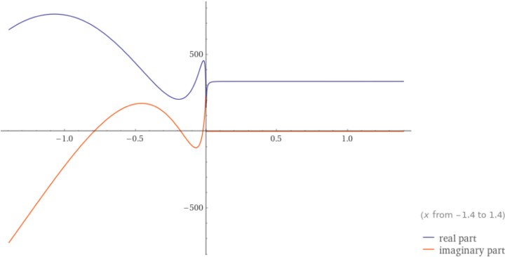
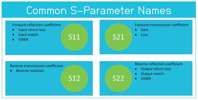
Complex Value Plot
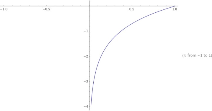
Logarithm Functions
Rohde & Schwarz
Electronic Instrumentation
Instrumentation refers to the field involved with testing and measuring electronic equipment and other mechanical or electronic items. It refers to the test instruments such as voltmeters, oscilloscopes, and spectrum analyzers as well as the large automated test systems used for mass testing and measuring of other devices. Instrumentation refers to data acquisition systems, medical tests and measurements, and a wide range of other products.
Excerpt from: “Electronics Explained: Fundamentals for Engineers, Technicians, and Makers” by Louis E. Frenzel. Scribd.
Read this book on Scribd: https://www.scribd.com/book/350143320
AXIOM Breakdown
Introduction by Art.S 04/10/2021 Post COVID-19
How do we setup and analyze our testing circuit connections pin-by-pin on a chip?
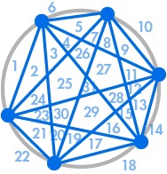
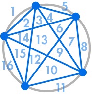
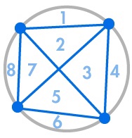
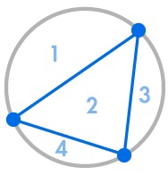
Imagine that we place several points on the circumference of a circle and we need to connect every point with each other.
This divides the circle into many different regions, and we can count the number of regions in each case.
The diagrams below show how many regions there are for several different numbers of points on the circumference.
We have to make sure that only two lines meet at every intersection inside the circle, not three or more. Art.S
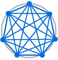
CASE=6 Totally Confusing Chart – right?
CASE=5 Confusing and Hard to Read Chart – right?
CASE=4 Confusing However Readable Chart – right?
CASE=3 A bit less confusing chart – right?
CASE=2 Much less confusing chart – right?
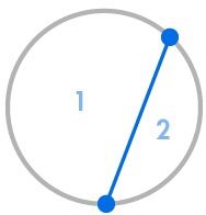
CASE=1 A Simple chart – right?

CASE=0 Not it all confusing chart – right?
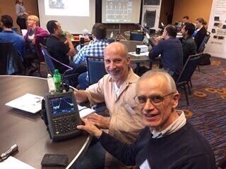
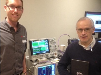
Equipment Certification Daily Routine
Equipment certifications are performed on most manufacturing, testing and production equipment to verify that the equipment is operating within the specifications defined in the production process.
Performing the certification on a daily routine
Performing the certification on a routine basis provides documented verification that equipment is meeting the specified requirements and is vital in maintaining confidence in quality assurance programs.
ICM SI engineering is skilled in providing me with equipment certification on Biological Safety Cabinets (BSC), Laminar Flow HEPA Workstations, Fume Hoods, compounding isolators and other equipment that has specific user requirements.

ICM SI engineering is highly trained and usually assist me with testing, repairs and qualifications of equipment to the manufacturing specifications and the applicable standards.

THE ENVIRONMENT CHECKS:

HEPA Filter Integrity
HEPA Filter velocity
Airflow Visualization
Viable Air Sampling
Viable surface Sampling
Temperature and Humidity uniformity
IQ/OQ/PQ
Laboratory Calibration Daily Routine
Calibrations are performed to analyze, determine, and rectify the graduation of any instrument giving a quantitative measurements.
Performing AXIOM Calibrations on an instrument
Performing calibration on a routine basis will help maintain instrument accuracy, producing results within the specified value and reducing the potential for errors– which also reduces manufacturing costs.
Performing Calibration on instruments provides documented verification that the instrument complies with the design specifications and user’s requirements, supporting the reliability of the instrument our lab offers in-house laboratory calibration services. Additionally, ISO 17025 calibration is available on temperature, humidity and pressure.
ESD
*
What is a ESD ?
ESD is defined as the sudden transfer of electrical charge between objects at different electrostatic potentials [1, 2] Also called Zap.
What is a ZAP ?
A cause of sudden moves of rapidly charged particles in a specific direction
HBM
The first one is the Human Body Model (HBM), which simulates the direct contact of a charged human body and a component.
CDM
The second is the Charged Device Model (CDM), which simulates the contact between a charged component with another component.
The major difference between these two models is the rise-time and the fall time of the ESD current pulse.
The HBM current waveform has typically a rise-time less than 10 ns and fall time between 50 and 300 ns.
The CDM current waveform has typically a risetime and fall time below 1 ns and 10 ns respectively [10].
ESD is defined as the sudden transfer of charge between objects at different electrostatic potentials [1, 2]. Electrostatic discharge can change the electrical characteristics of a semiconductor device, degrading or destroying it. Electrostatic discharge also may upset the normal operation of an electronic system, causing equipment malfunction or failure.
Electrostatic charge is created whenever two different materials comes into contact and are then separated. Creating electrostatic charge by contact and separation of materials is known as “triboelectric effect”. It involves the transfer of electrons between materials. The atoms of a material with no static charge have an equal number of positive (+) protons in their nucleus and negative (-) electrons orbiting the nucleus. For example, a person walking across the floor generates static electricity as shoe soles contact and then separate from the floor surface. The charge is transferred between objects normally via a spark when the potential across the narrowing air gap is high enough to cause breakdown [3, 4].
It is obvious that ESD is a transient overvoltage pulse with a steep rising edge, a high current amplitude but low energy content. A considerable amount of effort has been made to study ESD current waveforms and it has been shown that the amplitudes and risetimes vary with
Standard EN 61000-4-2, ESD generators, ESD
the charging voltages, approach speeds, electrode types and humidity [5-7].
A wide variety of engineering models have been proposed to simulate electrostatic discharge events but in general they fall into two categories [8, 9].
Rules for the protection strategy of an integrated circuit
During the design of the global ESD protection strategy of the IC, the ground rules are:
Rules for the protection strategy of an integrated circuit
Rules for the protection strategy of an integrated circuit
Rules for the protection strategy of an integrated circuit
During the design of the global ESD protection strategy of the IC, the ground rules are:
– each pin must have at least one ESD protection, with the exception of selfprotected pins;
– there must be a discharge path between all of the couples of the pins and for different polarities, positive and negative.
Another aspect involves the sizing of the protection, as well as its placement and associated routing:
– the sizing of the protection is conditioned by the value of its on-resistance RON. The silicon footprint of the protection depends in part on the targeted ESD robustness, keeping in mind the impact of the operating temperature on the value of RON;
– the resistors in these protections are usually made of polysilicon to avoid the formation of any parasitic components. However, it is important to size them correctly, making sure that the current capability does not become the weak link of the protection;
– the same precaution must be applied to the metallic rails whose routing must be as short and simple as possible, so as to avoid the effects of high current densities and of localized thermal heating;
– the placement and number of contacts and vias must also be carried out carefully, checking their respective current capability;
– in digital technologies, the ESD pads are already available, and placement is therefore pre-imposed. In mixed and analog technologies, each new circuit requires a new approach for protection.
Careful attention must be paid to the placement of ESD protections to avoid the formation of parasitic structures with certain blocks of the circuit;
Excerpt from: “ESD Protection Methodologies: From Component to System” by Marise Bafleur. Scribd.
Read this book on Scribd: https://www.scribd.com/book/354928445
Waveform and Signal Analysis
Understanding oscilloscope basics is critical to almost all product design.
What exactly is an oscilloscope, anyway? Quite simply, an oscilloscope is a diagnostic instrument that draws a graph of an electrical signal. This simple graph can tell you many things about a signal, such as:
Nearly all consumer products today have electronic circuits. Whether a product is simple or complex, if it includes electronic components, the design, verification, and debugging process requires an oscilloscope to analyze the numerous electrical signals that make the product come to life.
The Oscilloscope’s Graph
- The time and voltage values of a signal.
- The frequency of an oscillating signal.
- The “moving parts” of a circuit represented by the signal.
- The frequency with which a particular portion of the signal occurs relative to other portions.
- Whether or not a malfunctioning component is distorting the signal.
- How much of a signal is direct current (DC) or alternating current (AC).
- How much of the signal is noise and whether the noise is changing with time.
The Significance of Signal Integrity
A key benefit of an oscilloscope is its ability to accurately reconstruct a signal. The better the reconstruction of the signal the higher the signal integrity. Here’s one way to think of signal integrity. An oscilloscope is analogous to a camera that captures signal images that you then observe and interpret. Several key issues lie at the heart of signal integrity:
- When you take a picture, is it an accurate representation of what actually happened?
- Is the picture clear or fuzzy?
- How many accurate pictures can you take per second?
The Differences of Signal Integrity
The different systems and performance capabilities of an oscilloscope contribute to its ability to deliver the highest signal integrity possible. Probes also affect the signal integrity of a measurement system.
This primer helps you understand all of these elements so you can choose and use the oscilloscope appropriate for your application. Before you begin evaluating oscilloscopes, you need to understand the basics of waveforms and waveform measurements.
This information is covered in this chapter. It’s the foundation of putting an oscilloscope to work for you.
Understanding Waveforms and Waveform Measurementsy
The generic term for a pattern that repeats over time is a wave. Sound waves, brain waves, ocean waves,and voltage waves are all repetitive patterns. An oscilloscope measures voltage waves. A waveform is a graphic representation of a wave.
Physical phenomena such as vibrations, temperature, or electrical phenomena such as current or power can be converted to a voltage by a sensor. One cycle of a wave is the portion of the wave that repeats. A voltage waveform shows time on the horizontal axis and voltage on the vertical axis.
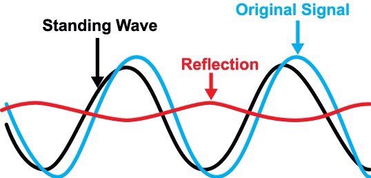
Waveform shapes reveal a great deal about a signal. Any time you see a change in the height of the waveform, you know the voltage has changed. Any time there is a flat horizontal line, you know that there is no change for that length of time.
Straight, diagonal lines mean a linear change; a rise or fall of voltage at a steady rate. Sharp angles on a waveform indicate sudden change. Figure 4 shows common waveforms.
Types of Waves
You can classify most waves into these types:
- Sine waves.
- Square and rectangular waves.
- Sawtooth and triangle waves.
- Step and pulse shapes.
- Periodic and non-periodic signals.
- Synchronous and asynchronous signals.
- Complex waves.
Next we’ll look at each of these types of waves.
Sine Waves
The sine wave is the fundamental wave shape for several reasons. It has harmonious mathematical properties”€it is the same sine shape you may have studied in trigonometry class.
The voltage in a wall outlet varies as a sine wave. Test signals produced by the oscillator circuit of a signal generator are often sine waves.
Most AC power sources produce sine waves (AC signifies alternating current, although the voltage alternates too; DC stands for direct current, which means a steady current and voltage, such as a battery produces.) The damped sine wave is a special case you may see in a circuit that oscillates, but winds down over time.
